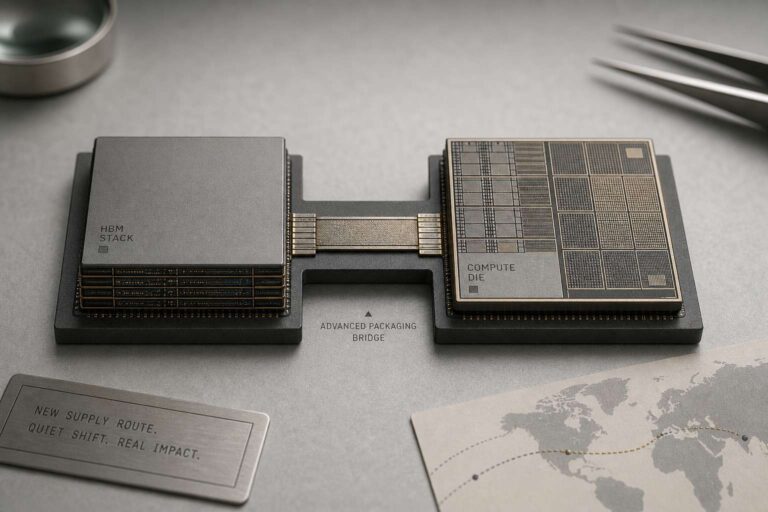
SK hynix is collaborating with Intel to use its Embedded Multi-die Interconnect Bridge, or EMIB, 2.5D packaging technology for HBM memory. The effort reflects SK hynix’s push to diversify its supply chain as customers increasingly consider Intel Foundry for advanced packaging. SK hynix is exploring research and development with Intel on 2.5D packaging technology to prepare its HBM memory for broader manufacturing options.
Intel’s EMIB interconnects multiple silicon dies using bridges embedded in a packaging substrate. SK hynix is interested in applying this technology to its HBM memory, with the apparent goal of bringing HBM4 memory modules in line with EMIB integration requirements. That would position the company to support partners developing next-generation Artificial Intelligence chips if they choose Intel Foundry for advanced packaging.
EMIB bridges are described as small silicon bridges available in variants such as EMIB-M with embedded MIM capacitors and EMIB-T with TSVs. These designs provide low-cost, high-density shoreline connections suited to logic-to-logic and logic-to-HBM interfaces. Until now, SK hynix has relied on TSMC and its CoWoS 2.5D packaging technology for this class of integration.
As CoWoS approaches its limits and customers look for alternative packaging methods, EMIB is emerging as a credible option for continued chiplet scaling. The technology is positioned to extend packaging flexibility in multiple directions beyond the traditional reticle limit of 830 mm² of silicon area. For SK hynix, the collaboration with Intel signals a practical effort to ensure its HBM roadmap can align with changing packaging preferences across the advanced semiconductor market.