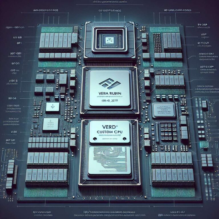
NVIDIA showed images of its Vera Rubin superchip system at GTC in Washington, D.C., presenting the first clear view of a two‑GPU Rubin assembly paired with a single Vera CPU in one package. The company quoted performance targets of roughly 50 petaFLOPS of FP4 compute per Rubin GPU, yielding about 100 petaFLOPS FP4 for the two‑GPU Superchip. NVIDIA said engineering samples are already in labs and set mass production goals for 2026 with broader shipments and deployments into 2027.
The pictures and brief specifications suggest each Rubin GPU integrates two reticle‑sized compute chiplets, potentially around 2 x 830 mm², paired with eight HBM4 stacks. That configuration delivers about 288 GB of HBM4 per Rubin GPU and roughly 576 GB of HBM4 on the full Superchip. The board also includes SOCAMM2 LPDDR5X modules to provide large, low‑latency system memory, and older briefings referenced roughly 1.5 TB of LPDDR5X per Vera CPU on typical trays.
The Vera CPU is described as an 88‑core, 176‑thread Arm‑based custom design and shows signs of a multi‑chiplet layout with a distinct I/O chiplet nearby. NVIDIA contrasted this approach with Grace, where the company had relied on Arm’s Neoverse designs, noting that with Vera the team developed the CPU core in‑house to extract maximum performance. The package appears intended to optimize tight CPU‑to‑GPU coupling for demanding workloads.
Interconnect and system bandwidth were highlighted as critical to the design. NVLink bandwidth climbs to approximately 1.8 TB/s to sustain heavy CPU‑to‑GPU traffic for system‑demanding tasks such as Artificial Intelligence inference and training. The combination of large HBM4 capacity, substantial LPDDR5X system memory, and a high‑bandwidth NVLink fabric positions the Vera Rubin superchip as a platform aimed at next‑generation data center deployments when broader shipments begin around 2027.