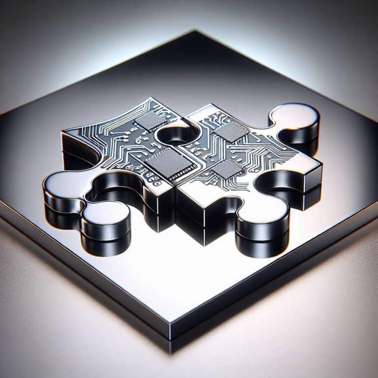
Marvell Technology announced what it describes as the industry´s first 2 nm 64 Gbps bi-directional die-to-die (D2D) interconnect IP, aimed at improving bandwidth and performance for next-generation XPUs and data center designs. The interface provides 32 Gbps in each direction over a single physical wire, enabling simultaneous two-way connectivity. Marvell said the IP is also available in a 3 nm version and is intended to meet scaling demands in high-performance compute environments.
The company highlighted several technical metrics to quantify the new IP´s advantages. Marvell reported a bandwidth density greater than 30 Tbps per square millimeter, which it said is more than three times the bandwidth density of UCIe at equivalent speeds. A minimal depth configuration is claimed to reduce compute die area requirements to 15% compared to conventional implementations. The interface also incorporates advanced adaptive power management that automatically adjusts device activity to respond to bursty data center traffic, reducing interface power consumption by up to 75% with normal workloads and up to 42% during peak traffic periods.
Marvell positioned the D2D IP as setting a new standard for performance, power efficiency, and resiliency for chip designers targeting XPUs and next-generation data centers. The announcement focuses on technical gains in bandwidth density, silicon area savings and dynamic power reduction as primary benefits for designers aiming to pack more bandwidth into smaller die areas. Availability timelines, pricing and partner or customer details were not stated. Not stated.