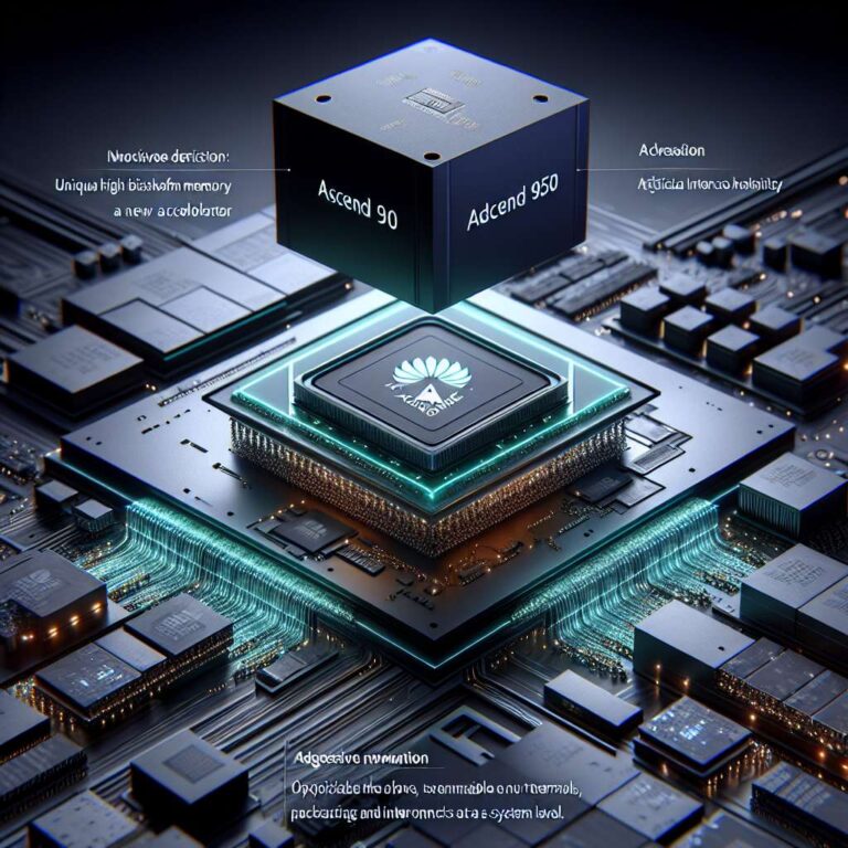
Huawei’s next-generation Ascend 950 artificial intelligence accelerator has been shown in detail for the first time, highlighting the company’s custom silicon and high bandwidth memory. The design combines Huawei’s first self-developed HBM with a new generation of artificial intelligence acceleration, signaling a strategy built around vertically integrated components and system-level optimization.
The Ascend 950 family is planned for early 2026 and will launch with two variants. The 950PR model includes 128 GB of in-house HBM with around 1.6 TB/s of bandwidth, while the 950DT model increases memory to 144 GB and boosts bandwidth to nearly 4 TB/s. Both chips target one PetaFLOP of FP8, and two PetaFLOPS of FP4, positioning them as high-performance accelerators even though Huawei currently trails NVIDIA in per-chip performance.
Huawei’s competitive approach centers on dense packaging and aggressive networking across clusters, aiming to win through scale rather than relying solely on raw per-chip metrics. Although the company has not confirmed the manufacturing process, the accelerator will likely use SMIC’s newest N+3 node with 5 nm-class features. Chinese SMIC has officially achieved volume production of its newest 5 nm node relying on the deep ultraviolet to manufacture its silicon, and since the first customer for N+3 was Huawei with the Kirin 9030 SoC, it is seen as logical that the Ascend artificial intelligence accelerator family would also be produced on the same node.