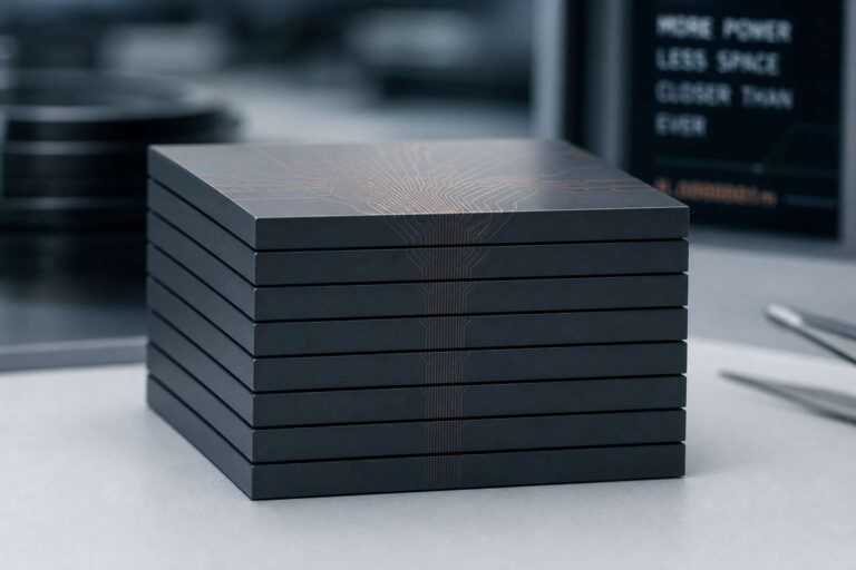
CEA-Leti announced a milestone in 3D integration, demonstrating a functional test vehicle using die-to-wafer hybrid bonding with pitches down to 1 μm. The findings were presented at the Electronic Components and Technology Conference (ECTC) 2026.
As Moore’s Law reaches physical limits, the semiconductor industry is increasingly turning to 3D stacking to improve performance and energy efficiency. The die-to-wafer approach is positioned to address a key bottleneck in Artificial Intelligence accelerator design: interconnect density and bandwidth.
By vertically stacking device layers with ultra-fine pitches, the technology shortens interconnect paths. That approach significantly increases data transfer speeds while reducing power consumption. CEA-Leti said the work is aimed at high-performance computing, advanced smart-vision systems, and Artificial Intelligence applications where dense, high-bandwidth interconnects are becoming more important.