Cadence has announced a major expansion of its design IP portfolio optimized for Intel´s 18A and 18A-P process technologies, accompanied by certification of its digital and analog/custom design solutions for the latest Intel 18A process design kit (PDK). The news was revealed at Intel Foundry Direct Connect, highlighting Cadence´s commitment to driving innovation in fields such as artificial intelligence, machine learning, high-performance computing, and advanced mobility through its strategic partnership with Intel Foundry.
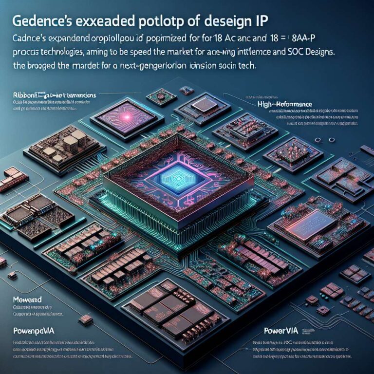
The core of this announcement is Cadence´s close collaboration with Intel Foundry, which has resulted in a suite of IP and tools tailored to exploit the unique features of the Intel 18A and 18A-P nodes. These nodes incorporate cutting-edge technologies such as RibbonFET Gate-all-around transistors and the PowerVia backside power delivery architecture. By leveraging these capabilities, the expanded Cadence solutions are designed to provide enhanced power, performance, and area (PPA) efficiencies, which are crucial for the development of next-generation system-on-chip (SoC) designs.
This collaboration aims to give joint customers the ability to achieve superior design outcomes and accelerate time to market for complex, high-performance applications. The expanded and certified portfolio underscores Cadence´s role as a key enabler for companies designing silicon targeted at innovations in artificial intelligence, high-performance computing, and emerging mobility sectors, while cementing the strength of their partnership with Intel Foundry.