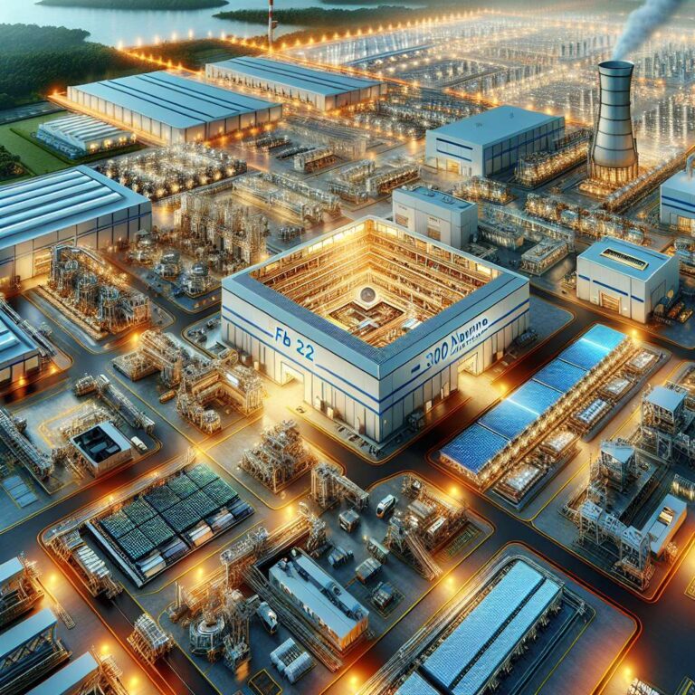
TSMC has announced that it has started 2 nm mass production in Fab 22 which is located in the southern city of Kaohsiung in Taiwan. The company notes that this is its first fab this far south in Taiwan and that Fab 22 represents the first phase of as many as five planned phases at this location. The facility is using 300 mm wafers and TSMC’s first-generation nanosheet transistor technology on the N2 node, positioning the site as a key hub for its most advanced process.
TSMC has already stated that the N2 node is offering a full node jump in terms of performance and power benefits, but the company is specifically comparing the N2 node to its second generation N3E node rather than the original N3 node, which suggests that the N2 node is slightly better than a regular full node improvement for TSMC. In addition to the nanosheet architecture, the N2 node also includes design and materials changes that aim to push performance and efficiency further than previous generations.
The N2 node also includes some new additions that TSMC claims will further boost performance, in the shape of a low-resistance redistribution layer (RDL) and super high-performance metal-insulator-metal (MiM) capacitors. The N2 node is said to offer a 10 to 15 percent performance increase at the same power consumption or a 25 to 30 percent reduction in power at the same performance, compared to the N3E node, as well as a transistor density increase of around 15 percent. Time will tell how these advancements translate into real world products, and which customers will be first to ship chips built on the N2 node from Fab 22.