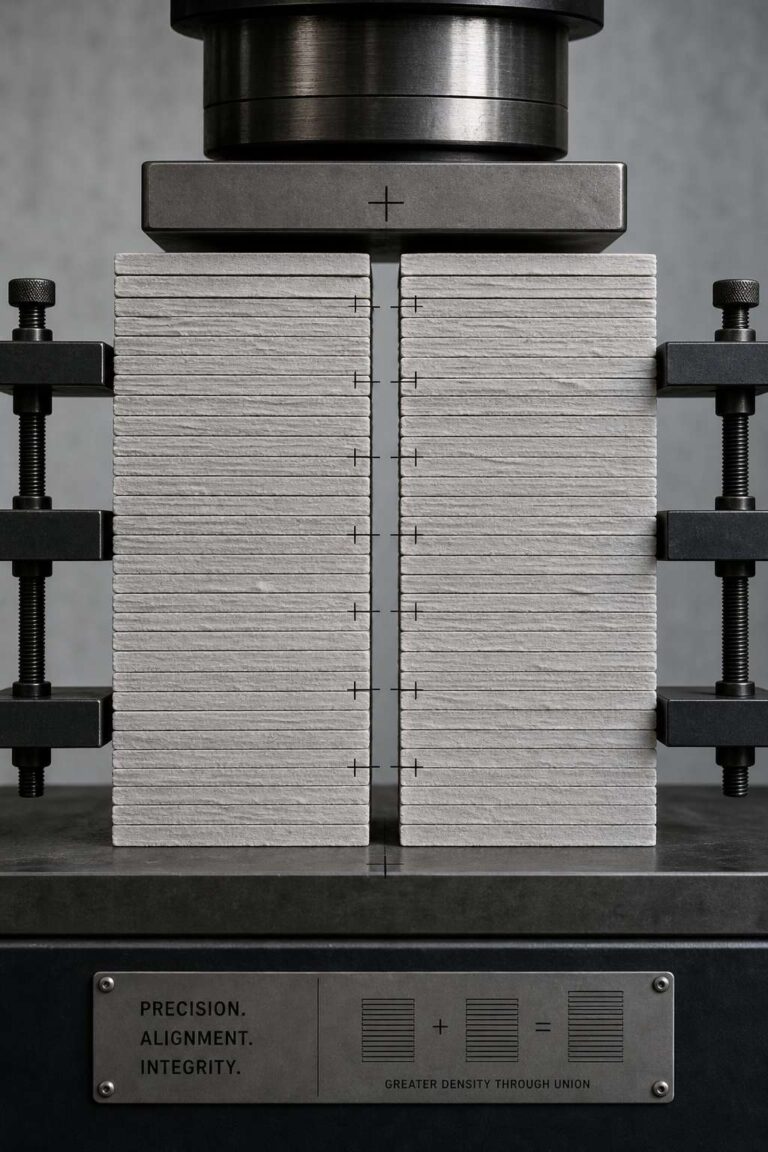
Samsung is advancing its NAND Flash roadmap by stacking two 450-layer V-NAND modules into a single 900-layer V-NAND chip. The company is pursuing this approach because manufacturing complexity makes it impractical to reach that density with a single chip. The design marks a packaging-led step toward Samsung’s goal of creating 1000-layer NAND Flash storage modules.
Samsung is using Cell Multi-Bonding (CMB) technology, a form of wafer stacking based on hybrid bonding. The process creates a permanent bond between two silicon chips through embedded metal bumps that are fused together to form a single chip. Multiple dies, or in Samsung’s implementation, multiple whole silicon wafers, can be connected by stacking two chip back ends together. Samsung’s proprietary CMB process paves the way for 1000-layer V-NAND chips by 2030.
Early last year, Samsung introduced its 10th-generation V-NAND technology, enabling over 400 layers on a single module. It also brought in hybrid bonding for the first time, suggesting the method has since matured. Moving to bonded 450-layer designs created manufacturing challenges because thick wafers are prone to warping.
To address those issues, Samsung developed microscopic chucks and new bonding techniques aimed at correcting overlay problems and misalignment during wafer bonding. Inside the NAND structure, the company also created new bitline and wordline designs to manage power consumption and keep individual chip sizes within a reasonable range. Together, those changes support Samsung’s effort to scale V-NAND beyond conventional single-die limits.