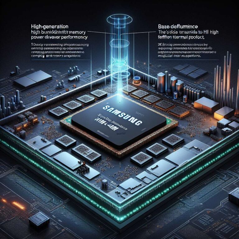
Samsung is preparing to apply its 2 nm process to the base die of HBM4E, the company’s 7th-generation high bandwidth memory, only a month after shipping the industry’s first commercial HBM4. The shift to 2 nm follows a redesign of the HBM4E power delivery network to handle an increase in power bumps from 13,682 to 14,457 within the same footprint, highlighting the growing electrical and thermal demands of next generation memory stacks. This evolution reflects a broader industry trend in which the base die is no longer a passive component and is instead becoming a critical logic element.
Up through HBM3, the base die primarily managed power and signal control at the bottom of the stack, but with HBM4 it began to take on some compute tasks directly, making the process node choice increasingly important. For HBM4, Samsung already used 4 nm logic base dies from its own foundry paired with its latest 1c DRAM, while SK hynix relies on a 12 nm (N12) process sourced from TSMC. Moving the HBM4E base die to 2 nm is intended to extend Samsung’s technical lead by improving power efficiency, thermal management, and area utilization, which are pivotal for demanding workloads such as Artificial Intelligence accelerators and high performance computing.
Competitors are also targeting custom HBM4E as a key battleground, with TSMC planning to use its 3 nm process for custom HBM4E and SK hynix developing its own versions. Standard HBM4E is expected mid-year, with custom product tape-in planned for the second half of the year, setting up a tight development race among major chipmakers. The move to produce HBM base dies internally on the 2 nm node also supports Samsung Foundry’s strategy by keeping fab utilization high and positioning the node as a cornerstone for ramping production at the Taylor fab in Texas, where equipment installation is underway and the first wafer tape-in is targeted before year-end.