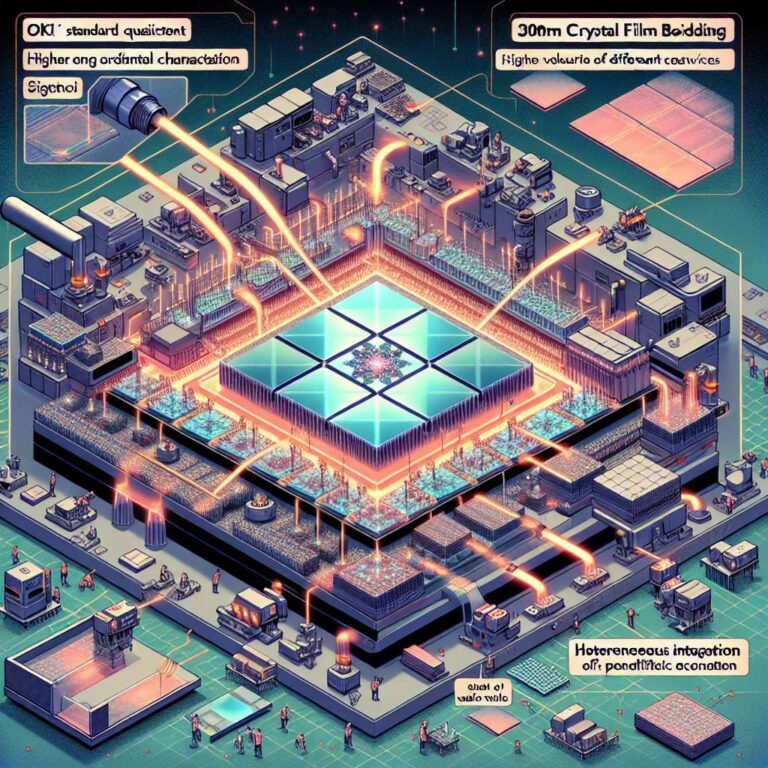
OKI has announced a new tiling crystal film bonding technology built on its proprietary CFB process that enables the heterogeneous integration of small-diameter optical semiconductor wafers onto 300 mm silicon wafers. The company says the method overcomes the long-standing wafer size restriction that prevented direct placement of smaller optical substrates on large-scale silicon wafers. OKI is positioning the development as a practical step toward higher-volume, integrated photonic-electronic devices and intends to move toward early commercialization in partnership with companies and universities.
The timing matters because rapid advances in Artificial Intelligence are driving explosive demand for data centers and raising a contentious social issue: how to expand data processing capacity without proportionally increasing power consumption. Photonics-electronics convergence is one candidate solution, offering high-density, high-speed transmission with lower energy per bit than purely electronic links. Heterogeneous integration of optical semiconductors with silicon photonics promises improved performance by combining specialized optical emitters and detectors with silicon´s mature processing and routing capabilities. OKI´s tiling CFB aims to make that integration compatible with 300 mm manufacturing, which is the industry preference for scaling and cost reduction.
Technically, the tiling CFB process lets multiple small optical dies or wafers be bonded in a tiled layout across a single 300 mm silicon wafer. That approach preserves the characteristics of the original optical materials while enabling placement at wafer scale for downstream processing and testing within standard silicon foundry flows. The method could improve yield economics by allowing selective use of functional optical chips and by leveraging large-wafer handling, alignment, and packaging techniques already established for 300 mm silicon.
Beyond the technical proof of concept, OKI is focusing on ecosystem work. The company plans collaborative trials and pilot runs with partner firms and academic labs to validate reliability, thermal behavior, and integration with silicon photonic circuits. If adopted, tiling CFB could influence supply chains for data center interconnects, telecom modules, and other systems seeking denser, lower-power optical links. The development is incremental rather than disruptive; nevertheless, it removes a key barrier to scaling heterogeneous photonic-electronic devices to mainstream silicon manufacturing.