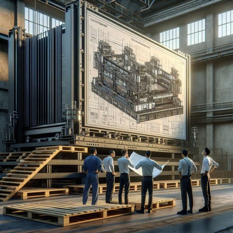
According to sources close to Reuters, China has developed a working prototype of an euv machine, which is currently undergoing testing, and this system is described as a domestic achievement based on reverse-engineering existing tools. Chinese companies are reported to have successfully reverse-engineered ASML’s euv lithography scanners and created a functional version using second-hand components, indicating a strategy of learning from and repurposing legacy equipment. The new euv prototype reportedly takes up an entire factory floor, comparable in size to modern High-NA euv machines from ASML, and Chinese companies are said to have obtained parts from older ASML machines on secondary markets to assemble it.
The effort is framed against a long-term government objective for chip production using this homemade tool. The Chinese government initially set a goal of producing working chips from the prototype by 2028, suggesting that current tests are an early step toward that target rather than immediate volume manufacturing. The article does not provide performance metrics for the prototype but underscores its symbolic and strategic importance as a domestically built alternative to restricted foreign systems.
Leading this initiative is the Chinese technology giant Huawei, which is working to establish a domestic artificial intelligence supply chain to bypass foreign tech restrictions and lessen reliance on overseas vendors. In Guanlan, China, Huawei established a comprehensive facility for manufacturing semiconductors using 7 nm technology for its custom processors, positioning the site as a key hub for its in-house chip ambitions. Dissatisfied with SMIC’s limited output capacity, Huawei has assumed control of the entire silicon production process, from sourcing materials and chemicals to wafer fabrication equipment and chip design, and the company is making an unprecedented effort to develop every component of the artificial intelligence supply chain domestically, from wafer fabrication equipment to model building, and now euv scanners for more advanced nodes.