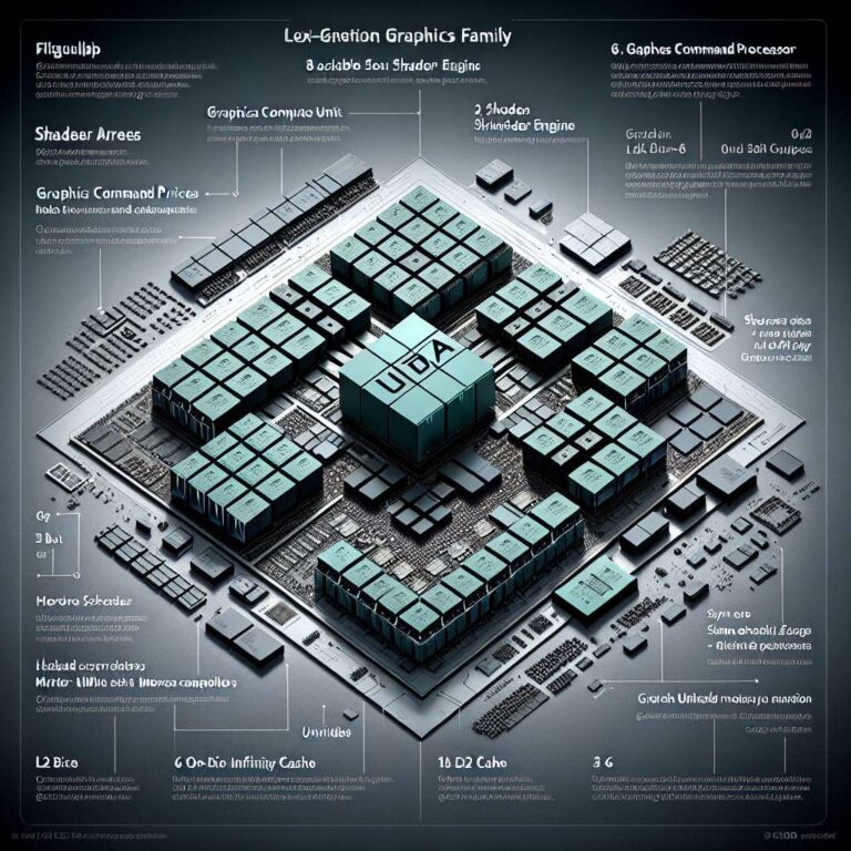
Leaked block diagrams from well-known hardware leaker Kepler_L2 sketch a modular next-generation AMD UDNA graphics family that could come in four die sizes, with the largest configuration rumored to top out at 96 compute units. The images depict repeating shader arrays and shader engines, with each engine containing multiple compute units and its own render backend. Those shader engines appear to feed into a central system-on-chip block that houses the graphics command processor, the graphics engine, hardware schedulers, and a shared L2 cache. On the memory side, the flagship diagram shows sixteen unified memory controllers, each listed as 32 bits wide, which would total a 512-bit external interface, and the leak also mentions a potentially much larger on-die Infinity Cache for the top-tier die.
Mapping the diagrams to specific configurations produces numbers consistent with the 96 compute unit claim. The flagship layout is described as eight shader arrays with two shader engines per array, yielding sixteen shader engines. At six compute units per engine, that configuration reaches the 96 compute unit figure. A mid-tier design reduces the scale to four shader arrays and eight shader engines with five compute units per engine, which works out to about 40 compute units and an estimated six memory controllers for a 192-bit memory bus. The leak further shows smaller designs with roughly 24 compute units and 12 compute units built from smaller arrays and fewer memory controllers.
One unusual detail is the 24 compute unit design being shown with as many as eight memory controllers, suggesting the controller widths could vary depending on whether the part uses a traditional gddr-style interface or an lpddr5x-like arrangement. Overall, the diagrams emphasize a highly modular architecture that can scale shader arrays, shader engines, compute unit counts, and memory controller counts across multiple die sizes. The details come from a rumor and leaked diagrams and should be treated as unconfirmed until AMD provides official specifications.