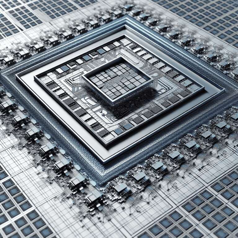
At its latest Technology Symposium, TSMC detailed an ambitious multi-year roadmap for its packaging technologies, emphasizing a dual-track strategy: Advanced Packaging and System-on-Wafer. Since the debut of CoWoS-S in 2016, where four HBM stacks were paired with N16 compute dies on a 1.5× reticle-limited interposer, the company has consistently raised packaging ceilings and interconnect capabilities. By 2025, CoWoS-S will support up to eight HBM chips with N5 and N4 compute tiles, all within a 3.3× reticle budget. The upcoming CoWoS-R will enhance interconnect bandwidth and add N3-node support while maintaining the same reticle area. Looking ahead to 2027, TSMC plans to introduce CoWoS-L, enabling large N3 chiplets, N2 tile integration, multiple I/O dies, and up to twelve HBM3E or HBM4 stacks under a 5.5× reticle—highlighting how what was once cutting-edge is now merely foundational, especially for forthcoming Artificial Intelligence accelerators by AMD and NVIDIA.
TSMC´s Integrated Fan-Out (InFO) technology takes packaging further with flexible 3D assemblies. The well-established InFO bridge already powers AMD’s Instinct accelerators, and updates like InFO-POP (package-on-package) and InFO-2.5D are set for release this year. These advancements will enable even denser chip stacking, breaking traditional 2D and 2.5D constraints and pushing into true 3D integration. This expansion provides new scaling opportunities for a single package and further supports the demands of rapidly advancing semiconductor designs.
Moving to the wafer scale, TSMC spotlighted its expanded System-on-Wafer (SoW) lineup: SoW-P and SoW-X. Initially developed for specialized Artificial Intelligence engines, these platforms now follow a roadmap aligned closely with the latest logic node progress. Notably, 2024 will mark the first implementation of System on Integrated Chips (SoIC) across N3 and N4 nodes, allowing each tile to reach 830 mm² with no fixed upper limit for the top die — a significant leap toward ultra-dense packaging. This trajectory aligns perfectly with the anticipated requirements of high-performance computing and Artificial Intelligence data centers as demand for computational density soars over the next several years.

