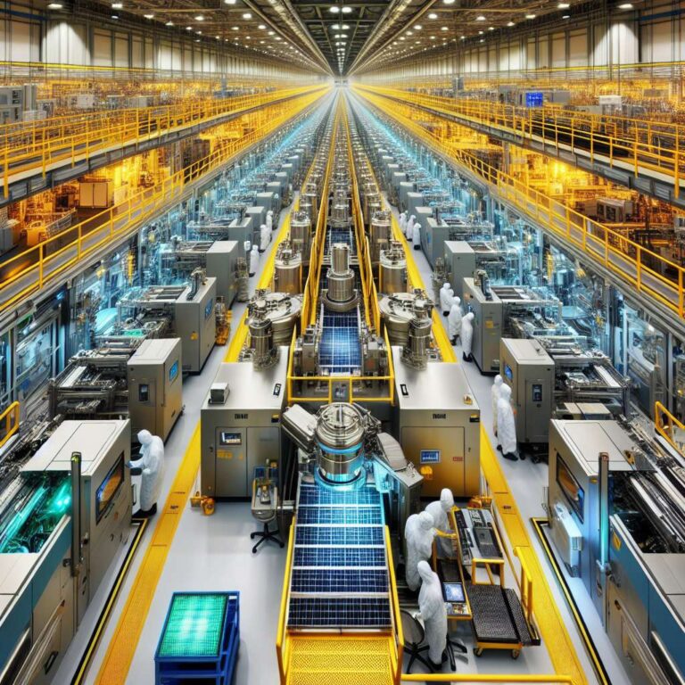
TSMC published a rare flyby video from inside Fab 21 near Phoenix, Arizona, offering an operational glimpse of the phase 1 cleanroom as it ramps production on N4 and N5 process technologies. The footage highlights hundreds of tools crafting chips for American customers and spotlights ASML Twinscan NXE extreme ultraviolet scanners that print the most complex layers for designs such as Nvidia’s Blackwell B300 processors. The video’s yellow-lit cleanroom underscores the strict photolithography controls, with lighting tuned to avoid unintended exposure of photoresists.
Early in the video, TSMC shows its automated material handling system, nicknamed the ‘silver highway.’ Overhead tracks move front-opening unified pods carrying 300 mm wafers, with hundreds of carriers in motion to orchestrate wafer logistics and sustain cycle times in a high-volume manufacturing environment. The film then zeroes in on EUV lithography, likely using ASML’s NXE:3600D systems, which create patterns with 13.5 nm wavelength light generated via laser-produced plasma from tin droplets. Purple plasma ignitions in the chamber are visible as part of this process. The piece notes the method’s challenges, including nanometer-scale overlay accuracy requirements (1.1 nm for NXE:3600D), stochastic effects, and the reliance on mirrors because traditional optics absorb EUV light. While wafer stages and pellicles are not shown, TSMC customizes these elements and employs them in Fab 21 phase 1.
At present, Fab 21 phase 1 is producing chips for companies including Apple, AMD, and Nvidia on N4 and N5 nodes. TSMC is also building Fab 21 phase 2, which the company says will be capable of N3 and N2-series process technologies, an acceleration from earlier plans that were tied to phase 3. Chief executive C. C. Wei recently told analysts that TSMC is preparing to move faster to N2 and more advanced nodes in Arizona to meet strong Artificial Intelligence-related demand. He added that TSMC is close to securing a second large piece of land to support expansion and enable an independent Gigafab cluster in the state for smartphone, Artificial Intelligence, and high-performance computing customers. TSMC defines a Gigafab as a site with more than 100,000 wafer starts per month.