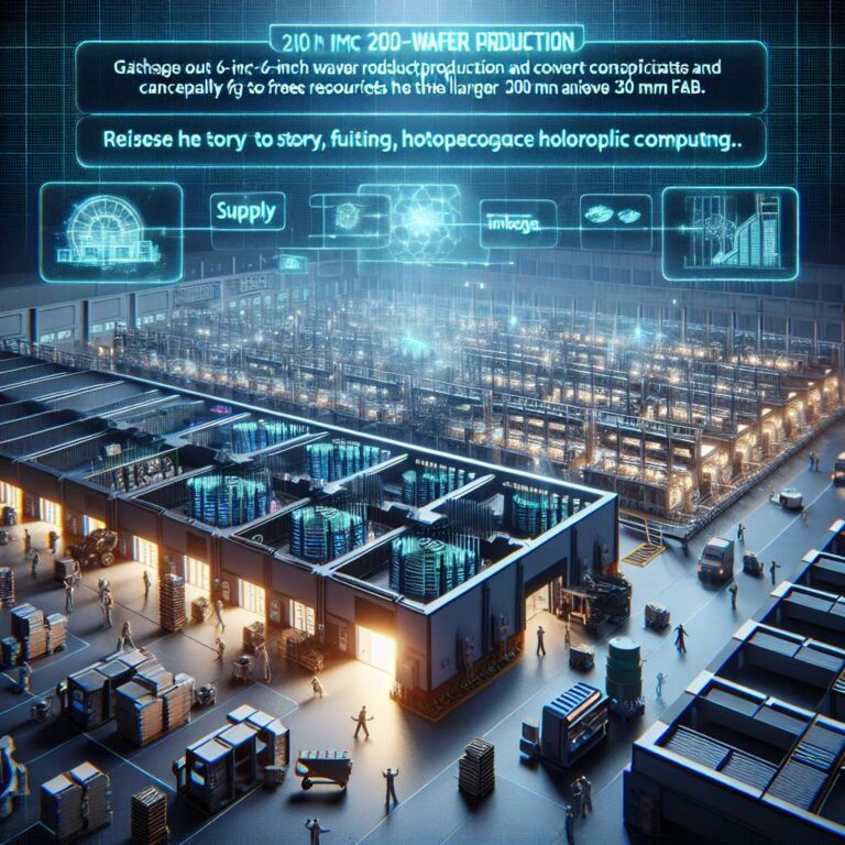
TSMC has announced a planned exit from 6-inch ´150 mm´ wafer production within two years and a consolidation of its 8-inch ´200 mm´ capacity as part of a wider cost and efficiency drive. The company is already winding down gallium nitride foundry services that depended on some 200 millimeter lines, and it intends to repurpose affected buildings in Hsinchu for other production or research uses. Taiwanese media have identified fab 2 and fab 5 as likely candidates to stop regular production by 2027, and TSMC says it will work with customers to migrate work to nearby 200 millimeter facilities while encouraging longer term moves to larger 300 millimeter gigafabs.
The business case is straightforward. Smaller wafers produce far fewer dies per cycle and cannot match the volume economics of modern nodes targeted at Artificial Intelligence and other high-performance markets. Consolidating older lines frees capital and talent, which TSMC will redirect into advanced node capacity and higher-utilization production at bigger fabs. The company pointed to continued emphasis on long-operating sites like fab 12 and on new construction across the street as parts of that shift, where larger wafers and higher throughput yield stronger returns.
Operationally, the change will be uneven. Some 200 millimeter factories can absorb displaced work, depending on tool compatibility and customers´ decisions. Other workloads will require negotiated ramp schedules, equipment redeployment, or migration of process recipes. TSMC has indicated it will cooperate with affected customers to minimize disruption, but companies with products designed around 150 mm platforms will face a shorter commercial runway and must plan transitions sooner than originally expected.
For suppliers and product teams the implications are concrete: fewer legacy cycles, potential redeployment of tools, altered demand for parts and services, and accelerated timelines for migration to 200 mm or 300 mm lines. The move signals a clear prioritization of scale and utilization over maintaining a broad array of small-wafer options, and it reshapes the near-term landscape for foundry customers working in older geometries and niche markets such as gallium nitride.

