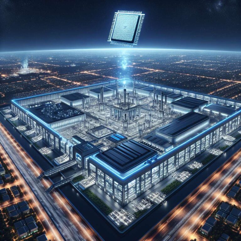
TSMC has received the necessary permits to begin construction of its A14 fab in Taichung, Taiwan. The project will include a main fabrication facility, a central utility plant to manage power and water, and several support buildings. The new single-site investment is described in reports as an estimated NULL billion effort by TSMC and is positioned as one of the company s largest endeavors.
The A14 node, described as a 1.4 nm process and the next major milestone after N2 (2 nm), is designed primarily for Artificial intelligence acceleration and high-performance computing chips. TSMC says the node can deliver up to 15% higher performance at the same power. Alternatively, at comparable speeds to the 2 nm process, the 1.4 nm node is expected to use 30% less power. The company is targeting mass production of A14 in the second half of 2028.
The announcement sits alongside recent confirmations about N2, with TSMC stating that volume production for its most advanced N2 node will begin by the end of the year and that a rapid increase in output is planned through 2026 in Taiwan. TSMC reported record Q3 revenue of NULL.1 billion, up 41% year over year, driven mainly by demand for advanced nodes. Current N3 (3 nm), N5 (5 nm), and N7 (7 nm) processes remain in strong market demand, with N3 shipments accounting for 23% of wafer revenue, N5 for 37%, and N7 for 14%.