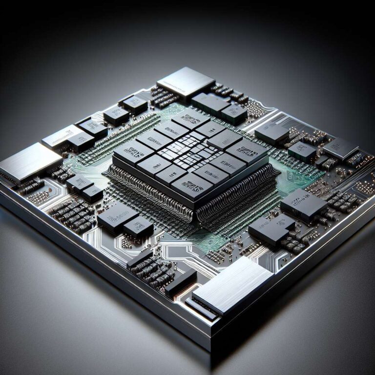
SK Hynix has showcased its most advanced high bandwidth memory, a 16 high 48 GB HBM4 module aimed at high capacity artificial intelligence and high performance computing accelerators that need large amounts of memory. This marks the first time SK Hynix has demonstrated a module that is more advanced than its earlier 12 high 36 GB HBM4, which used to run at 11.7 Gbps. For the new 16 high HBM4, there is no official data or speed reference yet, but the company presentation suggests that the four additional DRAM layers are intended to provide higher bandwidth for next generation accelerators.
The description of the 16 high HBM4 remained deliberately limited, which may reflect a competitive environment where Micron and Samsung are still refining their own HBM4 modules before supplying them to chipmakers such as AMD and NVIDIA. The wording of the announcement indicates that there is room for potential increases in speed if needed, signaling that performance targets may still be adjustable as ecosystem requirements become clearer. The focus for now is on capacity scaling and stack height rather than confirmed throughput figures.
Alongside the new HBM4 stack, SK Hynix also presented a custom base die HBM concept called cHBM. This design places a customized base die at the bottom of the DRAM stack that incorporates logic functions typically found on the GPU or ASIC logic die instead of in the memory itself. In SK Hynix’s demonstration, this includes features such as die to die PHYs, embedded memory controllers, HBM PHY, and related control logic, which can free up area on the GPU die for more compute logic and higher performance. The company emphasizes that customers can configure this base die to their needs and can even embed processing logic directly inside the die area to tailor memory subsystems more tightly to their accelerators.

