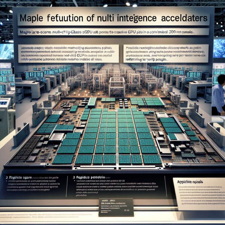
Japanese foundry Rapidus is positioning itself for stronger competition with TSMC by developing a panel-level packaging prototype based on a glass interposer, with the company planning to move towards mass production by 2028. The prototype, which will be showcased at SEMICON Japan 2025 in Tokyo, replaces conventional round silicon wafers with large square glass panels designed for high-performance artificial intelligence packages that combine multi-chip GPUs and more than a dozen of HBM dies. This strategy is presented as a way to reduce material waste and enable larger, denser multi-chip assemblies required for next-generation artificial intelligence accelerators without breaking the traditional laws of 300 mm wafer.
Rapidus is working on 600×600 mm glass panels, which are described as providing a significantly larger usable area than 300 mm silicon wafers and allowing more interposers to be produced from a single sheet. The company highlights that glass substrates can offer advantages in electrical performance and flatness when compared to organic package materials, making them attractive for dense interconnect structures. The shift from circular wafers to large square panels is also framed as an efficiency gain, as more packaging units could be patterned per panel, potentially lowering costs and improving throughput for complex chip assemblies.
At the same time, the article notes that glass introduces new manufacturing challenges, including fragility and potential warpage as panel sizes grow. These hurdles underscore why the technology is still at the prototype stage and why careful process development will be required before mass production. The article points out that Intel has notably discontinued its in-house development of glass substrates and instead has chosen to license the technology to others. The company can thus monetize its innovations, but large-scale Intel-based technology production is not anticipated until after 2030, suggesting that widespread deployment of glass substrate packaging across the industry remains several years away.