NVIDIA is reported to be the only major customer reserved for TSMC’s next-generation A16 process, planning to use the node for its upcoming Feynman GPUs. The company is lining up for samples in 2026 with volume ramps following in 2027, a schedule that would place Feynman after Rubin-class products built on refined 3 nm variants. If accurate, the move would make NVIDIA the sole large customer to adopt the A16 stopgap node between N2 and A14, while other customers are instead reserving N2 capacity or planning direct transitions to A14.
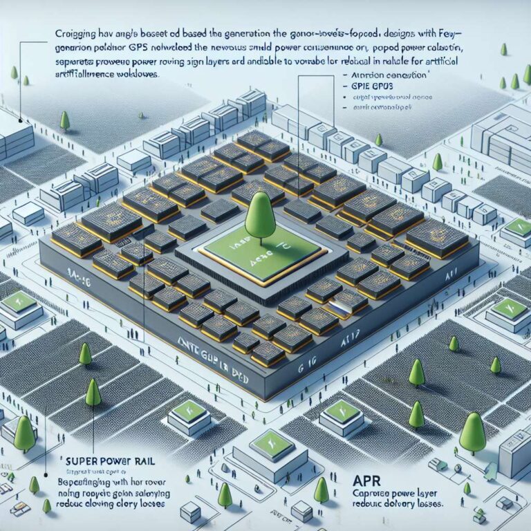
TSMC’s A16 is described as a nanosheet-focused design that incorporates enhanced backside power delivery, referred to in reporting as Super Power Rail (SPR). That approach separates power routing from signal layers to reduce delivery losses. The process is expected to deliver modest single-digit performance improvements, slightly higher transistor density compared with the previous generation, and more noticeable power reductions for Artificial Intelligence workloads. For very large dies and high-power cards, those enhancements can improve floorplanning, simplify thermal management, and increase the available capacity for memory and interconnect bandwidth.
Observers note that the A16 tradeoffs make it particularly relevant to datacenter and high-power accelerator designs, where power delivery and thermal behavior scale differently than in mobile parts. Companies such as Apple are reported to be reserving TSMC N2 2 nm capacity and plan to move to A14 as soon as it becomes available, effectively bypassing the A16 node for mobile and laptop designs in favor of less expensive N2 variants. For NVIDIA, however, the A16 improvements could provide practical benefits for next-generation datacenter chips even if the node does not deliver large raw performance leaps.

