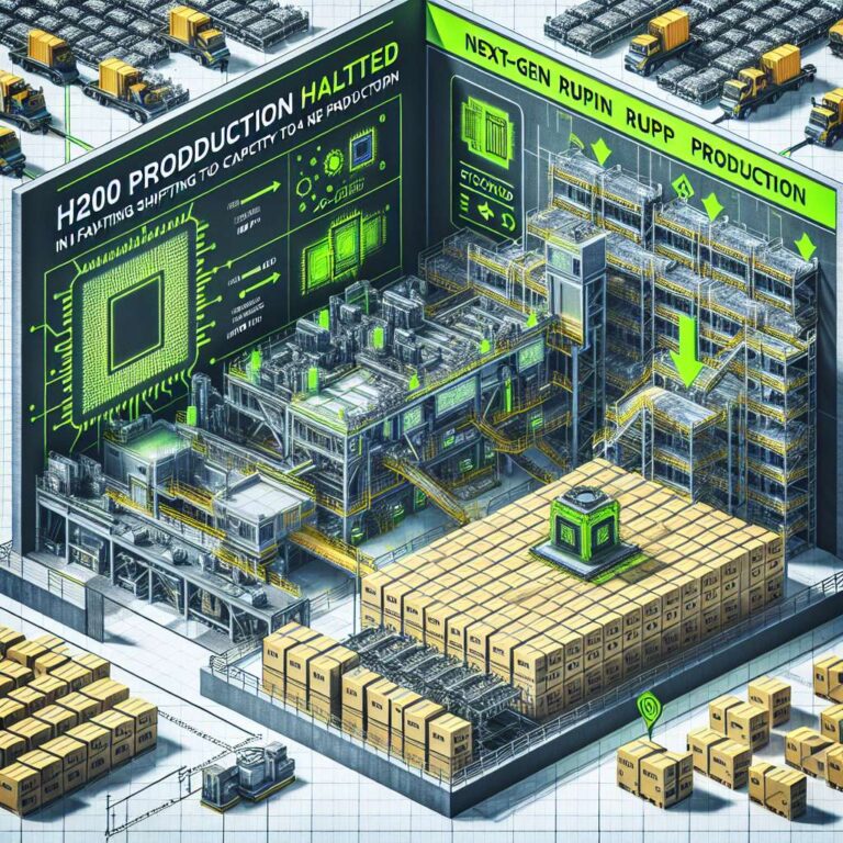
Nvidia has halted production of its China focused H200 Hopper GPU at Taiwan Semiconductor Manufacturing Company facilities after building a substantial buffer of inventory aimed at the Chinese market. The company has accumulated an inventory of 250,000 H200 GPUs, which will be available in the Chinese market for select applications that do not compromise United States national security. Nvidia began stockpiling these accelerators after securing export rights from Washington, intending to serve artificial intelligence laboratories across China while staying within tightened United States export controls.
Regulatory constraints on the Chinese side are now limiting how quickly this inventory can move. China has also restricted what its domestic companies and artificial intelligence labs can import, meaning that the import of H200 GPUs is still prohibited unless a company receives a letter of exemption from Beijing. As a result, Nvidia used its TSMC N5 5 nm node capacity to create about 250,000 units, which are now stored in a warehouse awaiting export approval from the U.S. administration and import approval from Chinese customs for artificial intelligence labs. This stockpiling strategy leaves Nvidia with a sizeable pool of ready hardware but dependent on dual government approvals before shipments can ramp.
Attention is now shifting to Nvidia’s next generation Rubin platform as production priorities evolve. The Financial Times and Reuters note that Nvidia will now “reallocate” capacity from H200 production to the new Rubin, even though the two generations differ in both process technology and packaging. For Hopper, Nvidia uses TSMC’s 5 nm node with CoWoS-S packaging, while Rubin uses a 3 nm node with CoWoS-L packaging. Analysts suggest these reports most likely refer to reallocating packaging or other secured capacity rather than directly converting mature 5 nm wafer lines, since it is unlikely that the 5 nm semiconductor node can be converted into a 3 nm node without significant line remodeling and changes to manufacturing equipment. Packaging can be adjusted more easily, which is likely the practical path for shifting resources from H200 to Rubin.