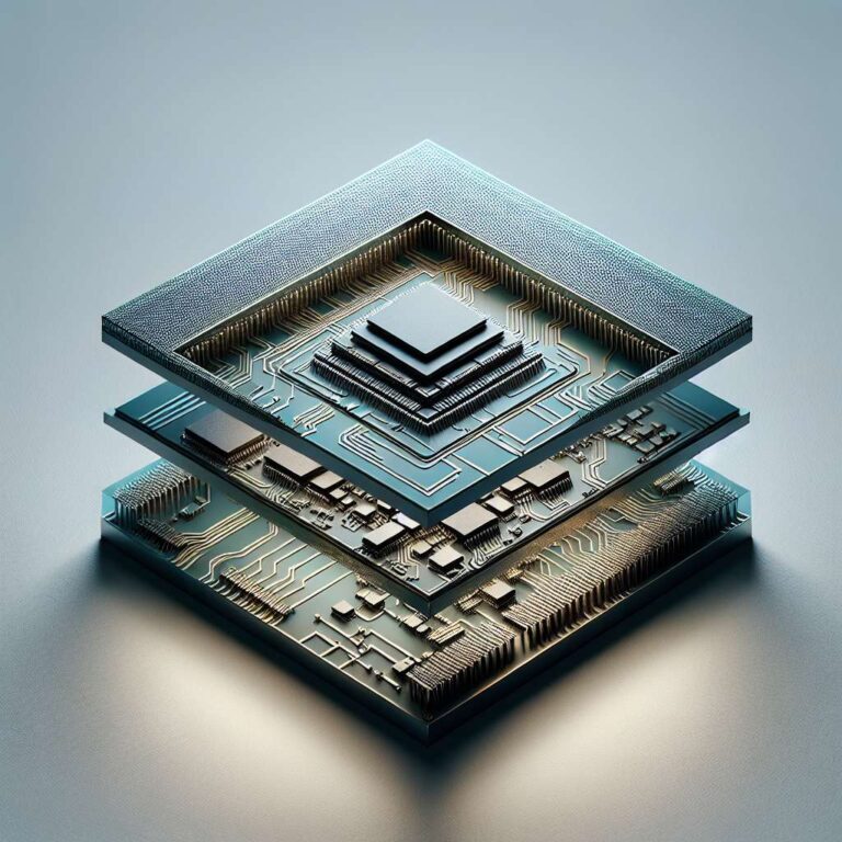
Intel has pulled back the curtain on its forthcoming 18A semiconductor process node at the VLSI Symposium in Japan, revealing advancements that position it as a significant leap over previous technologies. Scheduled for mass production in the latter half of 2025, Intel 18A integrates Gate-All-Around transistors with a PowerVia backside power delivery system, marking a dramatic shift in metal stack architecture design. By delivering power through the die´s rear, the company has freed up valuable front-side real estate, achieving tighter pitches for critical interconnect layers while relaxing constraints higher up. This reconfiguration not only boosts yield but also streamlines the overall manufacturing process.
Performance metrics from standardized tests using an Arm-based core sub-block showed approximately 15 percent higher throughput at equivalent power compared to the current Intel 3 process. If supply voltage is pushed to 1.1 volts, the node achieves up to a 25 percent clock speed bump with no increase in energy consumption. Alternatively, running at about 0.75 volts, chips fabricated on Intel 18A can realize an 18 percent performance uptick, or nearly a 40 percent reduction in power usage, offering remarkable versatility for everything from datacenter to edge deployments.
Underpinning these advantages are advances in physical design: cell heights have shrunk to 180 nanometers for performance-focused builds and 160 nanometers for density-optimized layouts, both improvements over earlier nodes. The number of front-side metal layers drops from as many as 19 in Intel 3 to a range of 11-16 in Intel 18A, complemented by three new rear metal layers essential for PowerVia. The company has further tightened interconnect pitches from 60 to 32 nanometers across primary layers. The adoption of low-numerical-aperture extreme ultraviolet lithography on key lower layers trims mask counts by 44 percent and cuts back complexity and cost. Intel intends to roll out 18A across a low-power ´Panther Lake´ compute chiplet and the forthcoming Clearwater Forest Xeon 7 series, spanning cost-optimized, balanced, and high-performance 17-, 21-, and 22-layer stack variants to meet the needs of diverse market segments, including future Artificial Intelligence hardware and advanced cloud platforms.

