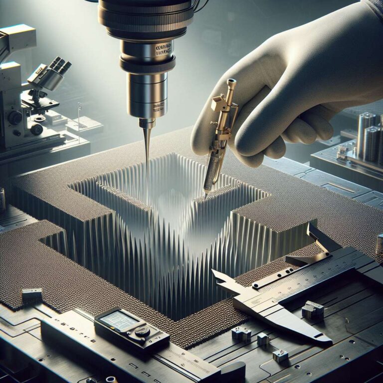
Forge Nano, Inc. announced a new atomic layer deposition process that it says fundamentally redefines the economics and architecture of advanced semiconductor manufacturing. The company has demonstrated high-speed, defect-free atomic layer deposition coatings in semiconductor features at a 1000:1 aspect ratio. Conformality is maintained at production-scale while providing coverage on features 2 orders of magnitude greater than line-of-sight techniques.
The company positions this capability as a way to remove a primary constraint that has limited 3D semiconductor scaling. By preserving conformal coverage in extremely deep and narrow structures, the process is described as enabling device architectures that were previously considered uneconomic or impossible. The focus is on unlocking more aggressive 3D geometries without sacrificing film quality or throughput.
The demonstration used production-representative wafers supplied by C2MI, a semiconductor process development and manufacturing innovation center in Canada. Conformality, defectivity and electrical performance were independently validated through C2MI’s internal metrology and reliability testing. Forge Nano presents this external validation as evidence that the process can be compatible with existing production environments while pushing aspect ratio limits significantly beyond conventional line-of-sight techniques.