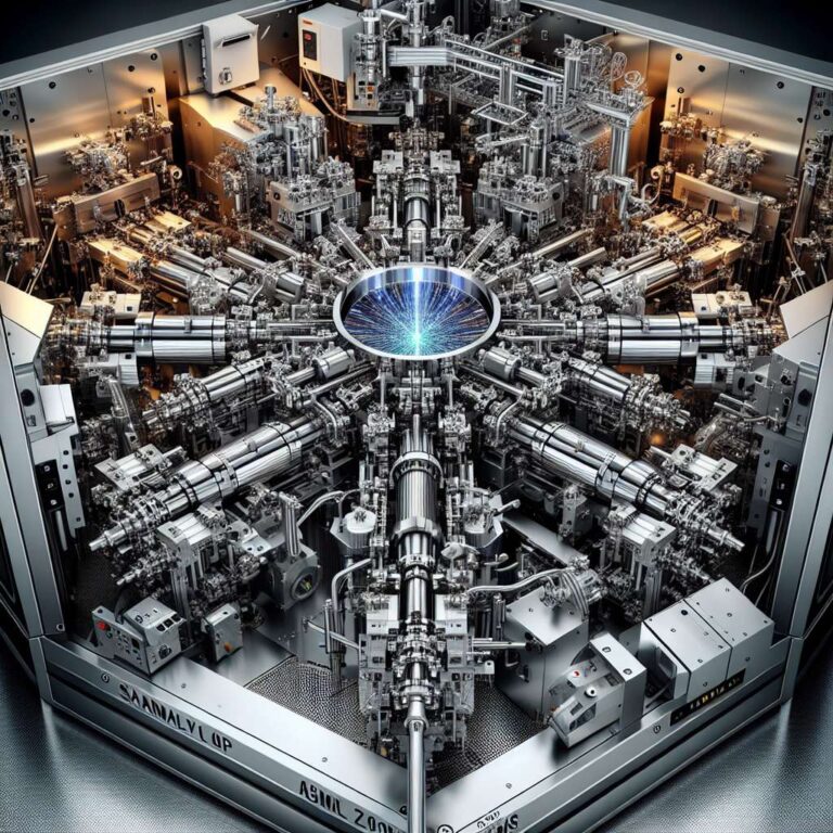
ASML has increased the light source power in its extreme ultraviolet lithography systems to 1,000 watts, up from roughly 600 W today, in a push to improve throughput and reduce chip manufacturing costs. According to the company, this boost in source power could enable up to 50% more chip output by the end of the decade. ASML says customers could process around 330 wafers per hour by 2030, compared to about 220 wafers per hour today, which would lower the cost per chip for advanced semiconductor production.
The extreme ultraviolet light, which operates at a 13.5 nm wavelength, is generated by firing a CO₂ laser at microscopic droplets of molten tin, creating plasma that emits extreme ultraviolet radiation. The emitted light is collected and directed through precision optics supplied by Carl Zeiss AG. To achieve the 1,000 W milestone, ASML doubled the tin droplet rate to roughly 100,000 per second and adopted a two-pulse laser shaping technique instead of a single pulse. The company states that there is a path toward 1,500 W and potentially even 2,000 W over time, signaling a roadmap for further throughput gains.
ASML remains the only supplier of commercial extreme ultraviolet scanners, which are used by leading chipmakers including TSMC, SK Hynix, and Intel, and are considered critical to advanced node production. These tools have also been subject to export restrictions to China, underscoring their strategic importance. The power increase is positioned as a way to maintain ASML’s technological lead while United States startups such as Pat Gelsinger’s xLight extreme ultraviolet venture and parallel Chinese efforts work on competing lithography systems. Chinese companies have reportedly been sourcing parts from older ASML machines via secondary markets, while Huawei is pursuing a homegrown artificial intelligence supply chain with a large semiconductor manufacturing facility in Guanlan focused on 7 nm chips for its own processors. The Chinese government had initially aimed to have a working prototype from this effort by 2028, highlighting the broader geopolitical race around advanced lithography.